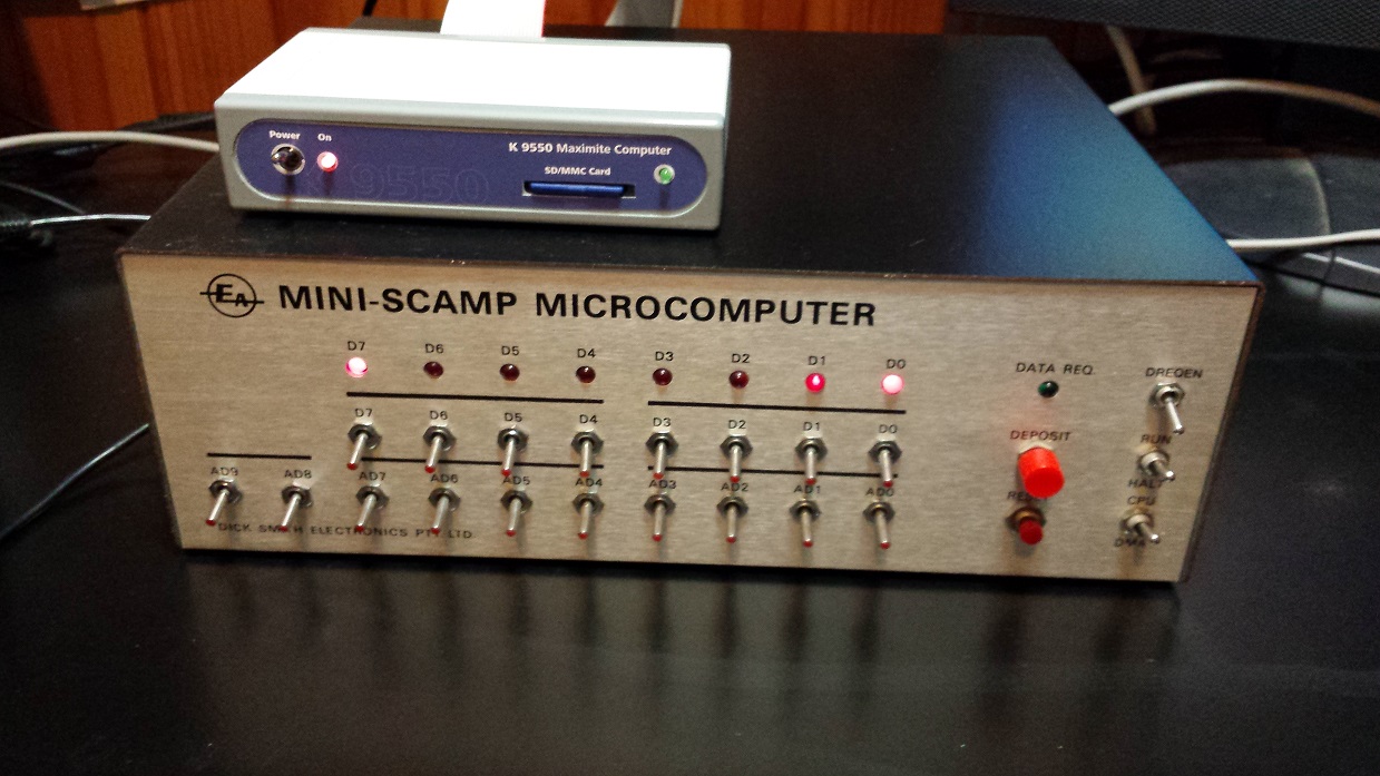
Like me, you may have a 1977 EA Miniscamp microcomputer tucked away. It is fun to get out every now and again, but it is very tiresome having to enter in the machine code via the front panel switches.
And also like me, you probably have a Maximite computer tucked into the same cupboard next to the Miniscamp.
This simple interface will allow the Maximite to drive the front panel switches of the Miniscamp, thereby allowing the tedious procedure of programming the Miniscamp to be programmed, and for those programs to be stored on the Maximite and quickly loaded into the Miniscamp.
But then, having done that, it opens the prospect of being able to program the Miniscamp for larger tasks. The Miniscamp kit was originally designed with only 256 bytes of RAM, and that is how mine has remained for the last 45 years. But with an old spare 6116 RAM chip, I will expand the memory from 256 bytes to a whopping 2kB which will allow the Miniscamp to run the original KITBUG monitor program.
That will leave one other essential upgrade, and that is to replace the ancient 110 baud 20mA serial current loop interface used by KITBUG with a modern USB serial interface so you can use a terminal emulator on your PC instead.
Background
The Miniscamp, published in Electronics Australia in 1977 provided a good introduction to computers, since it was a classic “lights and switches” design where you had to enter machine code directly into the RAM. This was possible with the SC/MP microprocessor which could be detached from the address and data buses and given to the front panel switches via the direct memory access (DMA) switch.
All the address and data switches are attached to open collector NAND gates which drive the bus. When the switch is open, the bus signal will be low and when it is closed, the bus signal will be high. (See figure 2 below).
The Maximite was the first iteration of a family of computers published more recently in Silicon Chip magazine which are all based on the BASIC interpreter developed by Geoff Graham. The Maximite provides 20 GPIO through as 26 pin DIL socket on the back of the computer.
This interface will connect these GPIO from the Maximite, configured as “open collector” outputs, to the NAND gates in the Miniscamp so that they can act as the switches (as long as the physical switches are open). And one of the GPIO outputs will also drive the write strobes to act as the “deposit” switch.
Maximite interface technical description
The interface uses all 20 I/O pins of the Maximite configured as digital outputs. There are 8 pins wired to the data switches and 11 pins wired to the address switches (allowing 2kb address range), plus 1 pin for the memory write strobe line. The interface is very simple without any active components; only a single diode on each pin (plus an additional one on the write strobe to provide two signals “WR1” and “WR2”). The outputs are normally held high, and are driven low to sink the TTL load from the Miniscamp’s address and data switch NAND gates. This has the same effect as if the front panel switch is closed, indicating a binary 1.
To fill memory on the Miniscamp, the Maximite will write 11 bits of the memory address to pin 12 (address bit 0) and pins 1 through 10 (address bits 1 through 10), and then write the 8 data bits to pins 13 through 20. The output of these pins is inverted, so that a zero is set for binary 1, and a one is set for binary 0. Then the write strobe (pin 11) is driven low momentarily to write the data to the selected address.
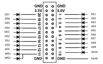
Figure 1 shows the wiring to the standard 26 pin Maximite interface. This shows the only additional components required to make this interface.
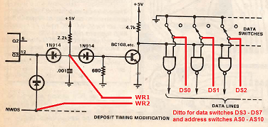
Figure 2 shows the interface points on the original Miniscamp circuit. The diode anode of each data and address line is wired to the same point in the circuit where the respective data switch or address switch connect to the TTL NAND gate. And the write signal is connected via two diodes. One will drive the ‘NWDS’ line low to enable the RAM write signal, and the other will trigger the RC circuit which enables the data switch NAND gates. Note that the circuit shown in figure 2 is taken from the “deposit timing modification” shown in the May 1977 publication; not the original April circuit by Dr. Kenwell. This is the design of the printed circuit board which was adopted in all the commercial kits.
Maximite interface construction
The DIL socket can be mounted on a piece of blank perforated board along with all the diodes as shown in the Photo 1. The 11 address and 8 data lines are wired onto the main PCB in parallel with the front panel switch connections (Photo 3), and the two write strobe signals are wired into the existing Miniscamp circuit at two points as shown in figure 2. One will drive the ‘NWDS’ line low to enable the RAM write signal, and the other will trigger the RC circuit which enables the data switch NAND gates. This piece of Veroboard is then simply mounted onto the back panel with silicone, as shown in Photo 2.
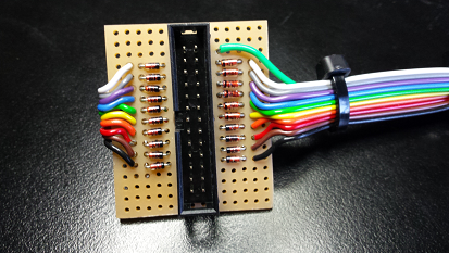
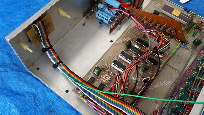
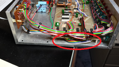
Photo 1 – The interface was simply constructed on a piece of blank perforated board. The diodes are wired directly between the DIL socket pins and the respective signal wires. There is also a green earth which will be connected to the chassis.
Photo 2 – The interface is held in place by silicone on the back panel behind the front panel LED driver PCB. The silicone provides a sufficiently solid mount without any other mechanical means.
Photo 3 – The data and address signals are wired directly into the underside of the main PCB where the front panel switches are terminated (circled above).
Maximite interface programming
scmp.bas is a BASIC program which will load the “binary count and display” test program from the original design article for the Miniscamp. Load and run this program on the Maximite while all the switches on the front panel of the Miniscamp are in the off position. It is satisfying and fun to watch the front panel LEDs blink as the program is loaded into memory when this BASIC program is run.
Then when the program has completed and the lights have finished blinking, reset the Miniscamp and place the DMA/CPU and Halt/Run switches into the CPU and Run positions. The program will start running.
RAM expansion technical description
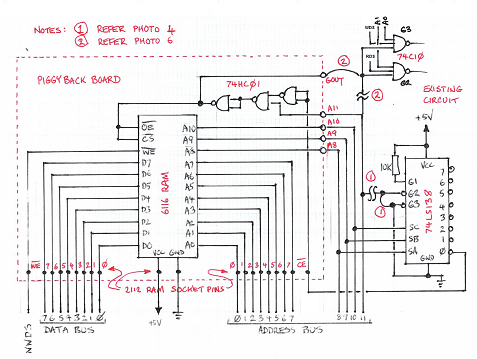
The KITBUG monitor program originally resided in a 512 byte PROM and occupied memory address 0000-01FF. But additionally, it stores variables on a stack in RAM at location 0FFF and below; in other words, it expects to have 4kB of addressable memory, but the memory expansion design presented here only provides 2kB (mainly due to the fact that I only had 6116 RAM chips, and the Maximite interface only provides a 2kB addressable range).
Additionally, the Miniscamp has the DMA input switches and and LEDs at memory address 0801 and 0802 respectively; right in the middle of the 4kB address space.
But this design provides a nice compromise to address all of these requirements. The 2kB of memory is mirrored in address ranges 0000-07FF and 0800-0FFF, although the first 256 bytes at 0800-08FF are disabled so as not to conflict with the Miniscamp DMA switches and lights. This means that all the existing Miniscamp programs can continue to run unmodified, whilst allowing the KITBUG monitor to have full access to the 2kB RAM and its stack.
To achieve this, pin G3 on the 74LS138 address decoder, which previously connected to AD11 so that the decoder is only active for the 0000-07FF address range, is instead tied to ground, so the decoder is active for both the 0000-7FF and 0800-0FFF range. And 74LS138 output “0”, which previously enabled the 2112 RAM chips in the 0000-00FF range, is gated with AD11 so that the 6116 RAM chip is disabled when AD11 is high and output “0” is low; i.e. address range 0800-08FF.
And the same signal which disables the 6116 RAM is also connected into the existing 74C10 3 input NAND gate, in place of address line AD11, so that the front panel switches and LEDs are enabled in this same address range, which is identical to the original Miniscamp design. So the new memory address map is;
- Address 0000-07FF: This is the full 2kB addressable range of the 6116 RAM
- Address 08×1: Front panel switches DMA input
- Address 08×2: Front panel LEDs DMA output
- Address 0900-0FFF: This is a mirror of address range 0100-07FF
RAM expansion construction
The memory expansion board I built piggy backs directly onto the 2112 RAM chip DIL sockets, and most of the data and address signals are acquired directly from these pins; in fact pins 13-16 of the 6116 RAM chip piggy back directly into 9-12 of one of the 2112 sockets to pick up data lines DB0-DB3. This can be seen in photo 5.
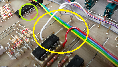
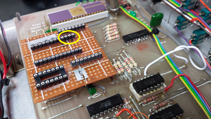
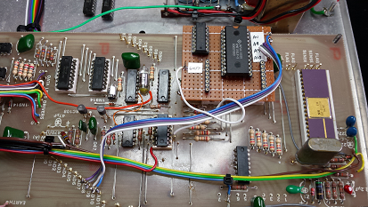
Photo 4 – Modifications to the main PCB include lifting pin 4 of the 74LS138 chip to disconnect it from address line AD11, and soldering it to adjacent pin 5 (circled in green above). And the wire link from pins 2 and 3 of the 74C10 to address line AD11 is replaced with a wire jumper (circled in yellow above). The Miniscamp will continue to operate with these modifications, and should be tested at this time.
Photo 5 – The memory expansion board plugs directly in place of the two 2112 RAM chips. Most of the existing data and address signals are brought up to this piggy back board directly from where it plugs into the IC DIL sockets, so there are only five additional signals which need to be wired from the board into the main PCB. Notice how pins 13-16 of the 24 pin DIL socket are configured directly above pins 9-12 of the 2112 RAM socket below on the main board. Then the two other 8 pin headers access all the other signals from the 2112 RAM sockets
Photo 6 – The RAM expansion board in place and populated with the 6116 RAM chip and the 74HC01 logic element. The wire link from the 74C10 (see photo 4) is disconnected from AD11 and connected to GOUT on this piggy back board instead. And the four address lines AD8-AD11 and wired to the main PCB.
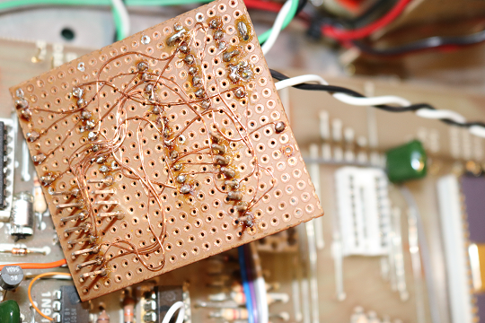
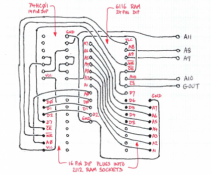
Figure 4 – This is the wiring on the underside of the piggy back board (viewed from the top). The solid circles in the DIP IC positions represent pins which plug into the 2112 RAM sockets. The open circles show all other DIP IC pins and the five external connections
Kitbug USB interface technical description and construction
Kitbug uses the FLAG0 and SENSEB pins on the SC/MP processor for serial I/O. The 20mA current loop interface can be simply replaced with a CP2102 USB serial module (available for a few dollars on ebay, etc.) by wiring the transmit/receive data signals directly to these pins, except that the FLAG0 output pin needs to be inverted. This is simply done by using the unused NAND gate of the 74HC01 chip in the memory expansion as an inverter.
| Address | 110 | 300 | 600 | 1200 |
| 0190 | 57 | 76 | A7 | 3D |
| 0192 | 04 | 01 | 00 | 00 |
| 019D | 7E | E5 | 45 | 76 |
| 019F | 08 | 02 | 01 | 00 |
| 01BC | 08 | 06 | 04 | 02 |
| 01C7 | FF | 64 | 25 | 86 |
| 01C9 | 17 | 06 | 03 | 01 |
| 01D3 | 8A | F0 | 50 | 81 |
| 01D5 | 08 | 02 | 01 | 00 |
The only other change that needs to be made is to alter the baud rate used by Kitbug from 110 baud to 300, since this is the lowest speed supported by the CP2102 module. This table shows the address vectors which need to be changed to do this, and you will notice that it can also be set to higher speeds of 600 and 1200 baud, but I have found 1200 baud to be quite marginal. And unless your Miniscamp has a crystal oscillator, you may even find achieving stable operation at 300 baud difficult. So if your Miniscamp only uses a capacitor for the timing component, you should probably consider replacing this with a 1MHz crystal or another stable timing method. (See appendix A of the SC/MP applications handbook for alternate methods).
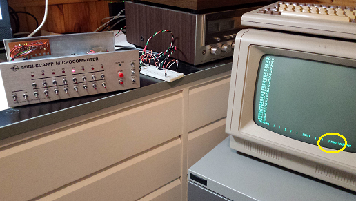
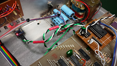
Photo 7 – The exciting moment when my Miniscamp ran KITBUG for the first time after 45 years. Notice that my ancient old ICL terminal (which has 20mA current loop) is running at 110 baud (circled on the screen).
To do this, I wired up the original transistor circuit for the 20mA driver on a prototype board and ran the unmodified 110baud kitbug.bas program on the Maximite.
Photo 8 – The CP2102 module is mounted on a pad of silicone at the rear of the Miniscamp, and it is wired, via the inverter on the memory expansion board back to the SENSEB and FLAG0 pins on the Miniscamp PCB.
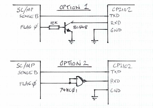
The serial output on pin FLAG0 is inverted in the original Kitbug driver and needs to be inverted for the CP2102 USB interface. Here are a couple of options to achieve this, although I used the second option, utilising the spare NAND gate on the RAM expansion board.
Using terminal emulators with Maximite and Miniscamp running Kitbug
My terminal emulator of choice is “PuTTY”. This terminal emulator does not provide any file transfer capabilities (although there are variants of PuTTY with file transfer extensions), but this is unnecessary when programs can be simply loaded into the Maximite using the AUTO command, which leaves you free to also use your favourite source editor of choice (mine in Notepad++).
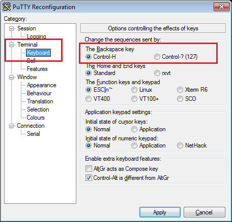
PuTTY is also a superior terminal emulator in all other circumstances. It works perfectly well with the Maximite because it provides ANSI/VT220 emulation as standard. You simply need to maximise the window when connected to the Maximite serial port so that it has more than 36 lines, and the change the default backspace keyboard encoding from chr(127) to Control-H. This is described in step 2b below.
Step 1 – Identify the serial ports
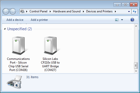
Step 1 – With both the Miniscamp and Maximite computers attached to your PC via USB, open the Windows Control panel (Devices and printers) to identify the serial port numbers that they have been assigned by Windows.
As you can see in this screenshot, the assigned port numbers are;
- COM26 – Maximite
- COM27 – Miniscamp
Step 2 – Connect to the Maximite
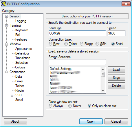
Step 2a Open a new Putty session. Select “serial” as the “connection type”, and enter the Maximite’s COM port number as the “serial line”.
Step 2b – You will also need to change the encoding of the backspace key which is chr(127) by default in the Putty emulator. To do this, select “Terminal > Keyboard” from the configuration categories, and change the backspace key setting to “Control-H”.
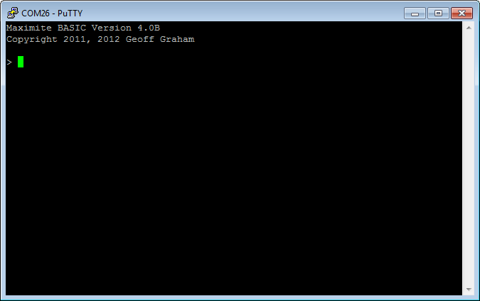
Step 2c – After clicking the “Open” button in the Putty configuration window, a terminal window will be opened to the Maximite and you should see the welcome message and prompt.
Step 3 – Connect to the Miniscamp

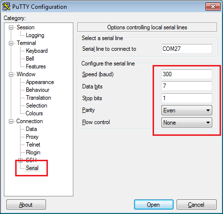
Step 3a – Open a new Putty session. Select “serial” as the “connection type”, and enter the Miniscamp’s COM port number as the “serial line”.
Step 3b – The Kitbug program was designed to operate with Teletype terminals which use 7 bit even parity, so you need to configure Putty the same. To do this, select “Connection > Serial” from the configuration categories and change the speed, data bits, parity and flow control accordingly.
Last steps – Load and run KITBUG!
Step 4 – Load KITBUG – After clicking the “Open” button in the Putty configuration window, a new Putty terminal window will open, but it will blank, since there is nothing running on the Miniscamp yet.
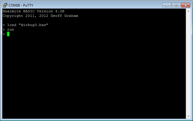
Instead, switch to the Maximite terminal window, load the kitbug3.bas program. See the steps below to save the program into your Maximite.
Before running it, you need to ensure that all the front panel switches on the Miniscamp are off (open circuit, zero state). Then “run” the program and watch the lights on the front panel of the Miniscamp blink as the progam is entered.
Step 5 – Run KITBUG – When the lights have stopped blinking, the Miniscamp will be loaded and ready to run Kitbug!
On the Miniscamp, press the “reset” button and set the DMA/CPU switch to CPU and the Halt/Run switch to Run.
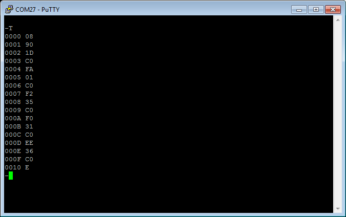
You should see a “-” prompt in the Miniscamp terminal window. Hit “T” then “Enter” and Kitbug will start to “type” the contents of memory. Hit “Enter” again and it will stop and print another “-” prompt.
See Chapter 4 of the SCMP Kit Users Manual for instructions to use Kitbug.
Saving 300 baud Kitbug to your Maximite
I have extracted the Kitbug machine code from it’s assembly code listing in the “Kitbug user manual” (using OCR! and lots of other tricks), and kitbug3.bas is the resultant BASIC program for the Maximite program which will load a 300 baud modified version of Kitbug into the Miniscamp.
But first of all, you will need to load this program and save it to the storage in your Maximite computer so it can be subsequently loaded and run. To do this, you will need to have a terminal session open to your Maxximite, as per step 3 above, then do the following;
- Open the kitbug3.bas into another window and press Ctrl-A and Ctrl-C to copy it into the Windows cut and paste buffer.
- In the Maximite terminal window;
- Enter the new command to erase memory
- Enter the auto command. Anything now type will be loaded directly into immediate program memory
- Click the right mouse button. This will paste the Kitbug progam from the Windows copy and paste buffer, thus loading it into immediate program memory
- Press Ctrl-C to stop the “auto” command
- Enter save “kitbug3.bas” to write the program to storage
Resources
- 4200079A_SCMP_Technical_Description_Jan76.pdf
- 4200094B_SCMP_Programming_And_Assembler_Manual_Feb76.pdf
- 4200113A_SCMP_Kit_Users_Manual_Mar76.pdf
- 420305239-001A_SCMP_Applications_Handbook-Feb77.pdf
- 420305365-001A_SCMP-II_Microprocessor_Retrofit_Kit_Jan77.pdf
- Kitbug source code
- Original 110 baud Kitbug loader for Maximite
- Putty terminal emulator download
- Miniscamp design articles
Comments are closed.